
The Complete IoT Product Development Process for Startups
 Wrirten by
Manaam Rehan
Wrirten by
Manaam Rehan
Transforming a unique connected concept into a physical, mass-manufactured market success is an incredible journey. Unlike traditional software app builds, hardware engineering requires managing physical materials, circuitry layouts, low-level firmware coding, and server-side data synchronization all at once. For emerging companies, navigating this multi-layered cycle without an organized roadmap can lead to expensive design updates and delayed timelines. Partnering with an expert product design company allows your venture to execute structural engineering systematically, accelerating your path from prototype to retail shelves. Here is an in-depth exploration of the complete engineering lifecycle for your upcoming launch.
Every engineering build begins by compiling a comprehensive Product Requirement Document (PRD). This core text acts as your technical North Star, defining battery targets, target price points, wireless connectivity boundaries, and exact operational environments. Locking in these precise boundaries early ensures your team develops targeted engineering paths, avoiding expensive scope creep that can quickly deplete an early-stage company’s foundational venture capital.
Once your product targets are set, industrial designers begin shaping your device’s visual style, user ergonomics, and physical footprint. Utilizing specialized industrial product design workflows, artists draft conceptual sketches and 3D computer models that match your target audience’s preferences. This phase balances pure physical styling with user mechanics, ensuring the housing looks excellent and feels completely natural in a user’s hand.
For a new venture, standing out in a crowded marketplace requires balancing aesthetics with manufacturability. Developing innovative product design for startups means designing physical housings that prioritize smart internal real estate layouts. Designers carefully calculate plastic draft angles, wall thicknesses, and internal mounting points early on, ensuring your exterior look functions beautifully while remaining simple and cost-effective to produce at the assembly factory.
Electrical architects begin by translating your PRD requirements into a fully realized functional block diagram, choosing microcontrollers, power regulators, and sensors. Through comprehensive product design services, engineers map out every complex electrical pathway and connection. This step ensures that all chips work together cleanly, preventing power rail overloads or data bus drops before moving into the physical board layout phase.
Connected products require specialized trace layouts to handle high-frequency radio waves without causing data signal drops. Implementing expert iot hardware design services means carefully routing antenna pathways and decoupling capacitors to isolate sensitive components from electrical noise. Proper shielding and component separation guarantee your Wi-Fi, Bluetooth, or cellular networks achieve maximum range while maintaining stable wireless cloud links.
Modern connected devices demand compact, multi-layer circuit layouts that maximize tracking efficiency within constrained spaces. Utilizing specialized pcb design services for iot devices allows engineers to create high-density interconnect patterns that minimize signal noise. This precision layout workflow ensures your circuit board integrates cleanly within your physical custom housing shapes, eliminating physical component collisions.
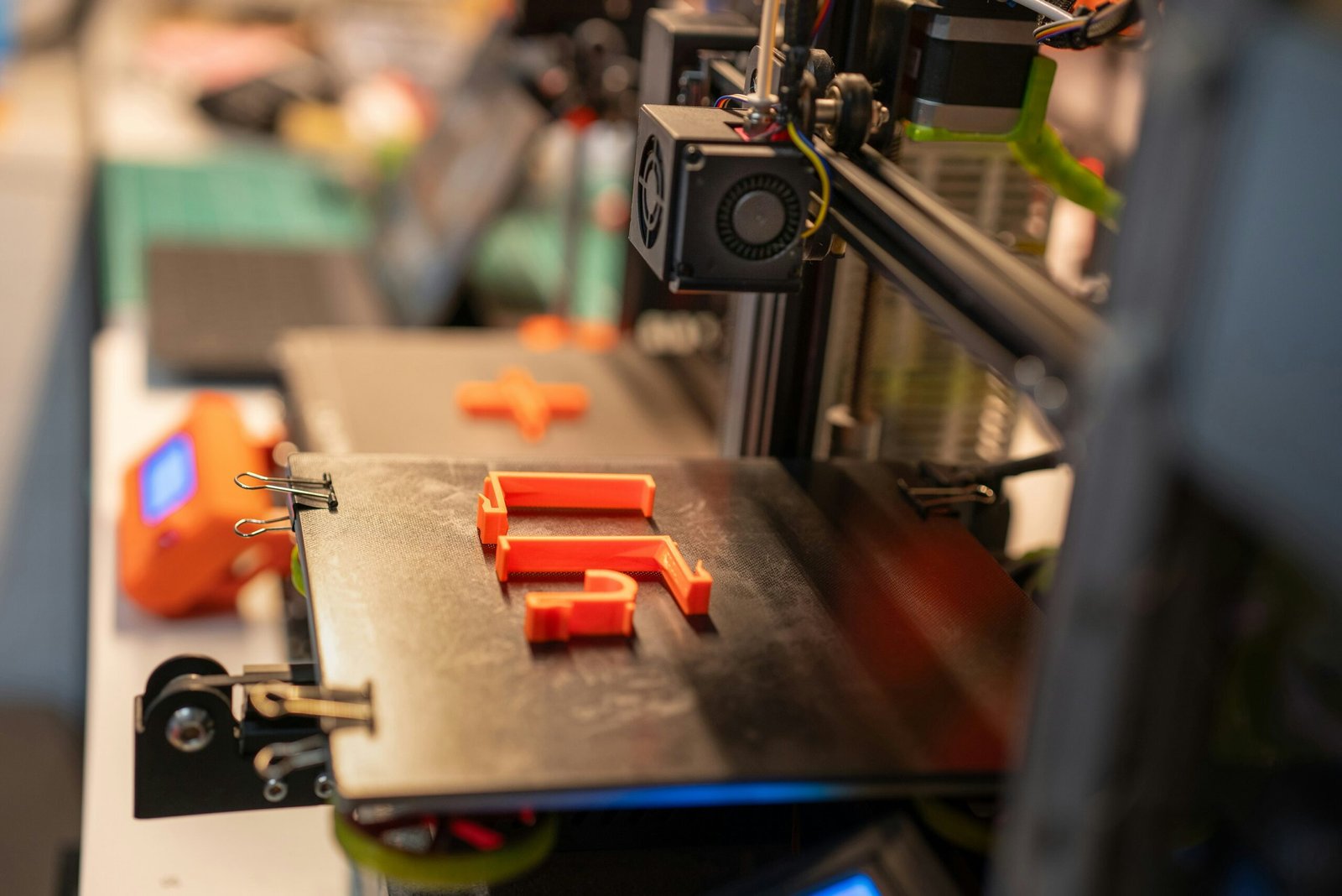
First-run prototype models are built using rapid tools like high-precision 3D printing and quick-turn circuit assembly. Combining these elements into product design and prototyping services workflows yields a functional, “works-like/looks-like” physical sample. Having these physical units allows your management team to test physical handfeel, check internal mechanical clearances, and discover layout anomalies early before starting mass manufacturing.
A freshly assembled prototype board remains completely inert until low-level software instructions are flashed onto its central microchip registers. Integrating professional firmware development services ensures your hardware drivers initialize perfectly, power-saving algorithms run smoothly, and local sensor telemetry is collected reliably. This low-level software code forms the bridge between physical silicon gates and high-level cloud communication platforms.
A major mistake for young ventures is hiring unlinked freelancers to build individual pieces of hardware, firmware, and housing models independently. Sourcing unified product development solutions through a comprehensive agency ensures all engineering fields communicate seamlessly. This team approach eliminates blame-shifting during initial board bring-up, accelerating troubleshooting cycles and saving thousands of dollars in prototype revisions.
Preparing for mass assembly requires optimizing every part of your design for automated factory machinery. Moving through custom product development for consumer goods steps means designing dedicated test fixtures to verify boards automatically on the factory floor. Engineers optimize assembly pathways, trace panel layouts, and pick-and-place orientation markers, protecting your production line from high assembly error rates.
Before your factory orders physical steel injection molds, engineers perform strict Design for Manufacturing (DFM) checkups on your files. This step modifies internal part intersections, strengthens mounting tabs, and eliminates fragile cosmetic structures. This disciplined review updates your engineering files, ensuring your modern product design can be assembled quickly with high production yields and minimal material scrap.
As your company scales from initial factory test batches to shipping thousands of units to global retail markets, your technology stack must remain highly stable and cost-efficient. Partnering with a proven product design consultancy provides your business with a long-term supply chain partner. They help manage factory quality checks, guide your hardware through regulatory compliance audits (like FCC or CE), and support your team across future product variations.

Q: What makes an innovative product design strategy successful for early-stage startups?
A: Success lies in designing a focused Minimum Viable Product (MVP) that utilizes pre-tested modular hardware components, allowing you to prove your market fit without spending excessive time and capital on over-engineered initial features.
Q: How do I find a reliable product designer who understands physical manufacturing limits?
A: Look for a dedicated product design firm with a verifiable portfolio of shipped, mass-produced consumer or industrial hardware items, rather than an independent rendering artist who only creates digital 3D models.
Q: Why should startups invest in affordable custom product design services instead of modifying cheap off-the-shelf development boards?
A: Off-the-shelf boards are physically bulky, consume excessive battery power, and contain unnecessary components that drive up unit manufacturing costs. Custom circuit engineering allows you to optimize the dimensions, extend battery life, and lower component costs for scalable commercial production.
Navigating the complex IoT product development process demands a balanced mix of industrial style, precise electrical engineering, secure wireless routing, and production-focused design discipline. By breaking your roadmap into structured phases—from initial PRD scoping to automated laboratory debugging and factory DFM refinement—you shield your venture from costly launch delays and product stability bugs. Do not cut corners on early physical validation. If you are ready to transform your connected product idea into a robust, high-yield commercial reality, contact our engineering group today to request an itemized technical development and manufacturing blueprint for your upcoming project.