Hardware & PCB Design

Custom hardware and PCB design for embedded and IoT products.

We design schematics, PCB layouts, power circuits, sensor interfaces, wireless hardware, and prototype boards for teams building real electronic products.

01
Tech Stack
Altium Designer KiCad EasyEDA Schematics PCB Layout Power Design Sensor Interfaces RF/Wireless Layout DFM BOM Review Prototype Testing

Hardware that is designed around the firmware, power, and real use case.

A good embedded board is not just a schematic and PCB layout. It needs the right MCU, clean power rails, reliable sensor interfaces, stable communication buses, debug access, manufacturable layout, and enough margin for real-world testing.

Services

01
PCB Design & Layout
PCB layouts for embedded boards, sensor devices, wireless modules, power sections, and compact prototypes. We design with routing, grounding, connector placement, test points, manufacturability, and bring-up in mind.
02
Schematic Design & Component Selection
We help select MCUs, sensors, power regulators, connectors, protection parts, radios, and supporting circuitry. Schematics are built for the required interfaces, power budget, firmware access, and prototype testability.
03
Prototype Hardware & Bring-Up Support
We support prototype validation after assembly: power rail checks, current measurement, programming/debug access, peripheral testing, sensor validation, and firmware/hardware fault isolation.
04
BOM Review & Practical Sourcing
We review BOM choices for availability, cost, package size, power consumption, firmware support, and alternate part options. This helps reduce redesign risk before PCB fabrication.
05
Hardware-Firmware Integration Review
We review the board from both hardware and firmware sides: boot pins, debug headers, reset behavior, ADC ranges, pull-ups, interrupt lines, low-power paths, radio placement, and production programming access.
Problems We Solve

Problems We Solve

Hardware issues usually appear during prototype testing: unstable power rails, wrong pin choices, noisy ADC readings, sensors that behave differently on the PCB than the dev kit, high sleep current, weak wireless performance, missing test points, or boards that are hard to flash and debug. We help catch and fix these issues before they become expensive redesigns.

How We Work

How We Work

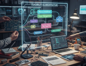
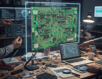
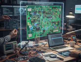
We start with the product requirements, power budget, wireless needs, sensors, enclosure constraints, and firmware access. Then we create or review the schematic, plan the PCB layout, prepare fabrication files, and support prototype bring-up after assembly. The goal is not just a board that looks complete, but a board that can be powered, programmed, tested, debugged, and improved.

Expected Results

Expected Results

You get a board design that is easier to build, program, debug, and validate. The deliverables can include schematics, PCB layout, BOM, Gerbers, assembly files, test notes, and bring-up support. For existing designs, we can review the board and identify practical fixes before the next revision.

Need help with hardware or PCB design?

Send us your requirements, existing schematic, PCB files, or prototype issue. We can help with new board design, design review, PCB layout, BOM review, and bring-up support.