
How Long Does Embedded Product Development Take?
 Wrirten by
Manaam Rehan
Wrirten by
Manaam Rehan
One of the most frequent questions stakeholders ask before launching a new smart device or connected system is: “When will it be ready for market?”
Because an embedded product lives at the intersection of custom multi-layer circuit boards, low-level firmware coding, mechanical enclosures, and strict global safety testing, there is no overnight solution. Developing a commercial-grade product in a rush almost always leads to unexpected component collisions, signal noise, and failed lab audits.
For a realistic commercial projection, an end-to-end embedded product cycle typically spans 6 to 14 months. Partnering with an expert hardware design company streamlines these phases, but understanding the timeline drivers keeps your budget and expectations anchored. Here is a realistic timeline breakdown from initial concept sketch to high-yielding mass production.
Before drafting schematic lines or laying down copper traces, your project requires a rigorous definition of its functional, economic, and aesthetic footprint.
Finalizing the Product Requirement Document (PRD): This phase establishes your technical foundation. Engineers define precise power targets, pick primary wireless protocols (like Bluetooth, Wi-Fi, or cellular), and calculate target manufacturing unit costs.
Shaping the Looks-Like Industrial Design: Industrial designers sketch and 3D-model the external enclosure, balancing modern styling with internal real estate limitations.
Executing Early Mechanical Design Reviews: Designers evaluate draft angles and uniform wall thicknesses early on. This preventative review ensures the outer shell can be cleanly formed later via high-pressure factory plastic injection molding tools without warping.
With a locked physical footprint, the technical team begins architecting the actual electronic brain and low-level software engines.
Schematic Capture and Component Selection: Electrical architects select microcontrollers, sensors, and power regulators, mapping out exact connection layouts through professional product design services.
Multi-Layer PCB Routing and Signal Integrity: Layout designers spend weeks routing complex, high-density tracks. Utilizing specialized pcb design services for iot devices, they isolate noisy digital high-speed paths from fragile analog sensor traces to prevent data packet corruption.
Writing the Foundation Firmware Architecture: Code architects develop custom hardware abstraction layers and low-level drivers, ensuring that sensor inputs register perfectly and power-saving algorithms maximize field battery life.
The project reaches a critical engineering milestone when digital blueprints are transformed into physical testing units for verification.
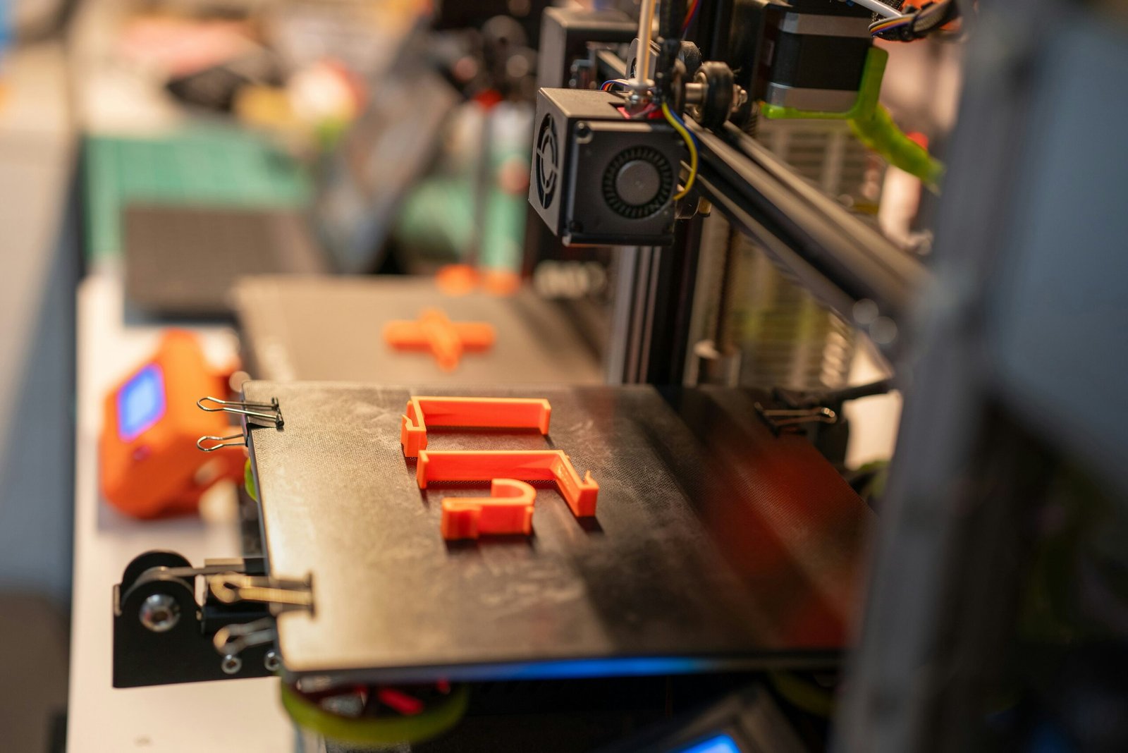
Fabricating Initial Engineering Validation Prototypes: Raw circuit boards are assembled using automated pick-and-place machinery, and custom housings are generated via high-precision 3D printing or CNC milling.
Systematic Laboratory Board Bring-Up: Hardware engineers subject initial samples to strict validation testing, using oscilloscopes and logic analyzers to eliminate voltage drops, signal distortion, or firmware bugs.
Iterating the Design Layout (The Re-Spin Phase): Almost every complex embedded device requires at least two to three prototyping rounds. Engineers use these testing loops to adjust component spacing, optimize radio frequency (RF) antenna matching, and iron out hardware-software bugs.
The final phase involves transitioning your validated, lab-tested prototype into a high-volume, commercially certified retail asset.
Cutting Steel Injection Molds and Final DFM Reviews: Factories analyze your mechanical files under strict Design for Manufacturing (DFM) rules before cutting heavy steel production molds, a process that takes 4 to 8 weeks on its own.
Clearing Global Regulatory Certifications: To legally sell your product, it must pass rigorous lab tests to secure stamps like FCC (United States) and CE (Europe). Working with an established product design consultancy ensures your grounding layouts are clean, allowing you to pass emissions audits smoothly on your first attempt.
Deploying Automated Production Testing Fixtures: Engineers design custom “bed-of-nails” factory testing jigs to check production quality instantaneously, allowing the factory assembly line to safely scale from pilot testing runs to shipping thousands of retail units.

Q: What is the number one cause of unexpected timeline delays in hardware development?
A: Supply chain oversights and late-stage component changes. If an engineer specifies a single-source chip that goes out of stock right before production, the team is forced into an expensive, multi-week board layout and firmware redesign.
Q: Can we accelerate our launch timeline by skipping the informal pre-compliance laboratory testing?
A: Absolutely not. Skipping pre-compliance scans to save an immediate week can backfire catastrophically. Failing a formal, binding FCC or CE exam can force your project back into a complete hardware redesign, adding months of delays and thousands in extra testing fees.
Q: How do pre-certified wireless modules impact our embedded development schedule?
A: Utilizing pre-certified Bluetooth or Wi-Fi modules dramatically speeds up the timeline. It cuts out weeks of complex RF tracking and antenna tuning during the layout phase, and permits a simplified regulatory approval path that shaves months off the compliance timeline.
The timeline for embedded product development is defined by the strict realities of physical manufacturing and global regulations. While a software app can be updated in hours, a flawed physical circuit board takes weeks to redesign, manufacture, and test anew. By following a structured timeline—from initial PRD scoping to disciplined prototyping loops and strict factory DFM reviews—you insulate your business from costly, late-stage redesign bottlenecks. Partnering with an integrated engineering agency that houses hardware, software, and mechanical disciplines under one roof removes communication friction and ensures your device hits retail shelves on schedule. If you are ready to build a reliable, market-ready connected device, contact our engineering group today to establish an optimized timeline for your upcoming project launch.